
- Sensor and networking excellence for Packaging, Food, Beverage, Pharma, and Personal Care industries
- Life Science
- Steel and Metallurgical Industry
- Efficient metalworking using sensor and automation technology
- Drive Technology
- Mobile Equipment
- Advancing battery manufacturing automation: Achieving superior efficiency and quality
- Automobile industry and suppliers
- Plastic Industry
- Energy Production
- White goods
- Electronics industry
- Tire Industry
- Traffic Engineering
- Intralogistics automation
- Robotic sensing: Precision and efficiency in robotics automation
- Automation in the semiconductor industry
- Components for hydraulics and pneumatics
Automation in the semiconductor industry
Precision for semiconductor, solar and display production
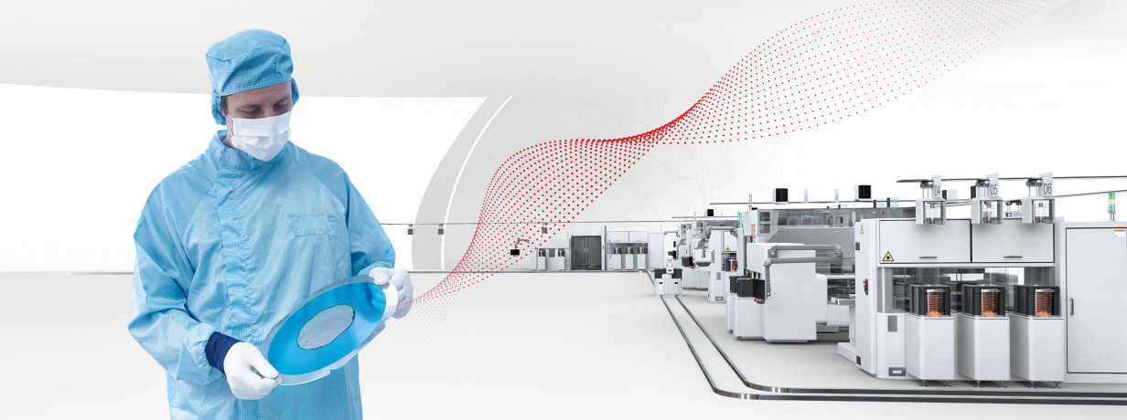
Mobile communication, Internet of Things, Smart Factories, Smart Homes - all these developments are driven by ongoing digitalization. At the heart of these technologies are semiconductors, which have become indispensable in industry as the main component of microchips. Demands placed on semiconductors are increasing with the digital transformation -- chips continually need to become more powerful. At the same time, a highly complex and technologically demanding process must be economically mastered to produce semiconductors.
Balluff offers you competent support for processing wafers in the chip and solar industry as well as for display production.
Automation solutions from Balluff for the semiconductor industry
Individualized and demanding requirements often require customized solutions. Our product range offers both standard solutions and customized solutions from our department of Customer Design & Engineering (CDE).
Exceptionally high process accuracy is guaranteed with our innovative and high-precision photoelectronic sensors with MicroSPOT technology. The sensor heads and the external processor unit can be easily integrated into your machines.
In addition, the special design features of certain sensors allow them to be used directly in a vacuum.
For space-critical automation applications, our portfolio also includes particularly compact yet powerful sensors.

The semiconductor industry is a critical cornerstone in today's world, driving innovation across various sectors. As Global Market Segment Manager, my goal is to constantly monitor developments in the market, understand your unique requirements in semiconductor manufacturing and thus ensure that our offerings bring the best results in all our use cases in this industry. Today we already serve customers from the semiconductor manufacturing segment in various areas such as wafer handling, wafer processing or carrier handling.
Benjamin Renz, Global Market Segment Manager, Semiconductors & Electronics
Spotlight applications in the semiconductor industry
Learn more about selected applications that give you an insight into how specific challenges in the semiconductor industry are solved reliably and with precision using Balluff components.
Further examples to suit individual areas of use
Discover how Balluff solutions ensure extreme precision in every critical process step of semiconductor manufacturing.
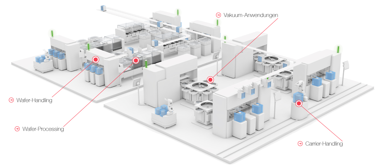
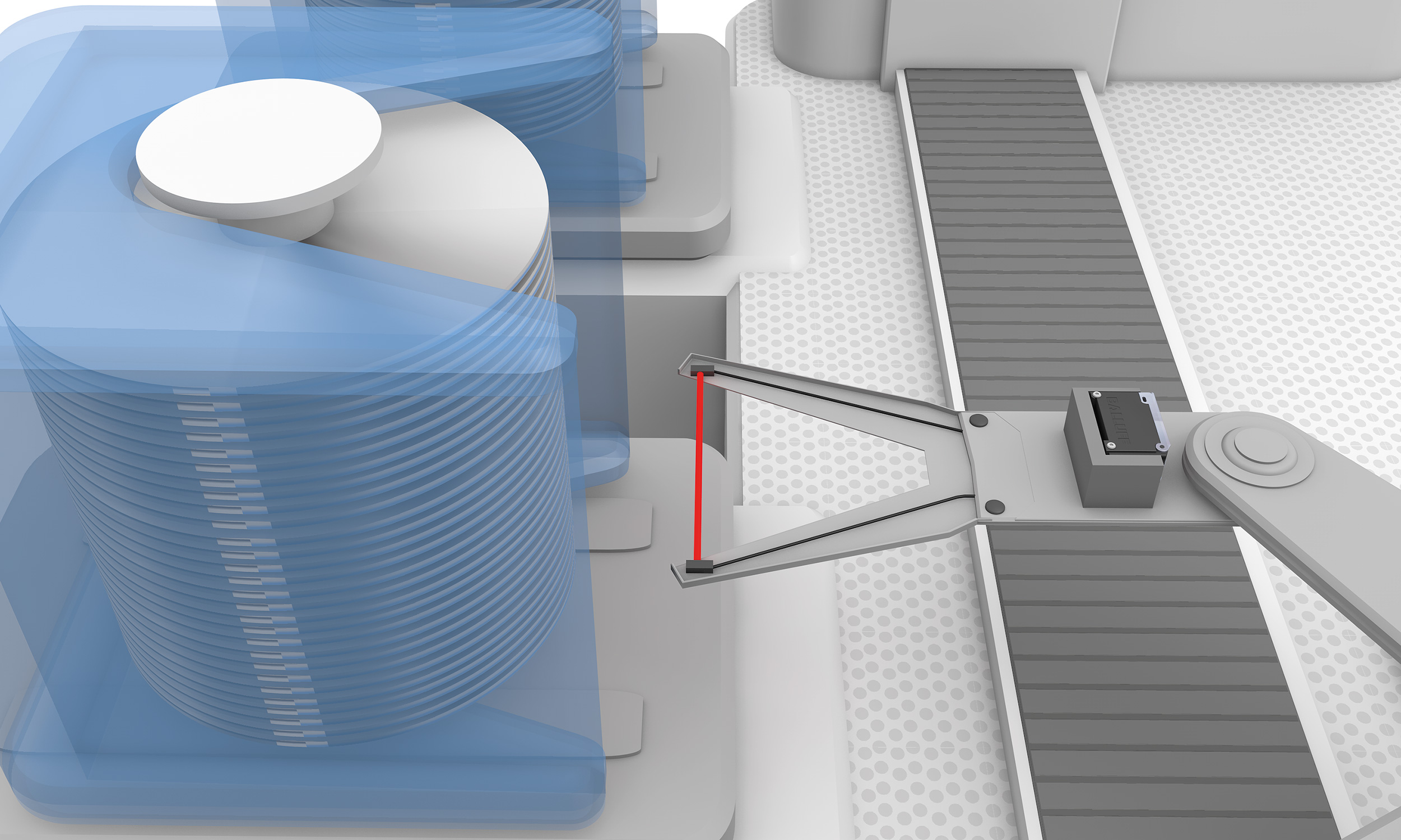
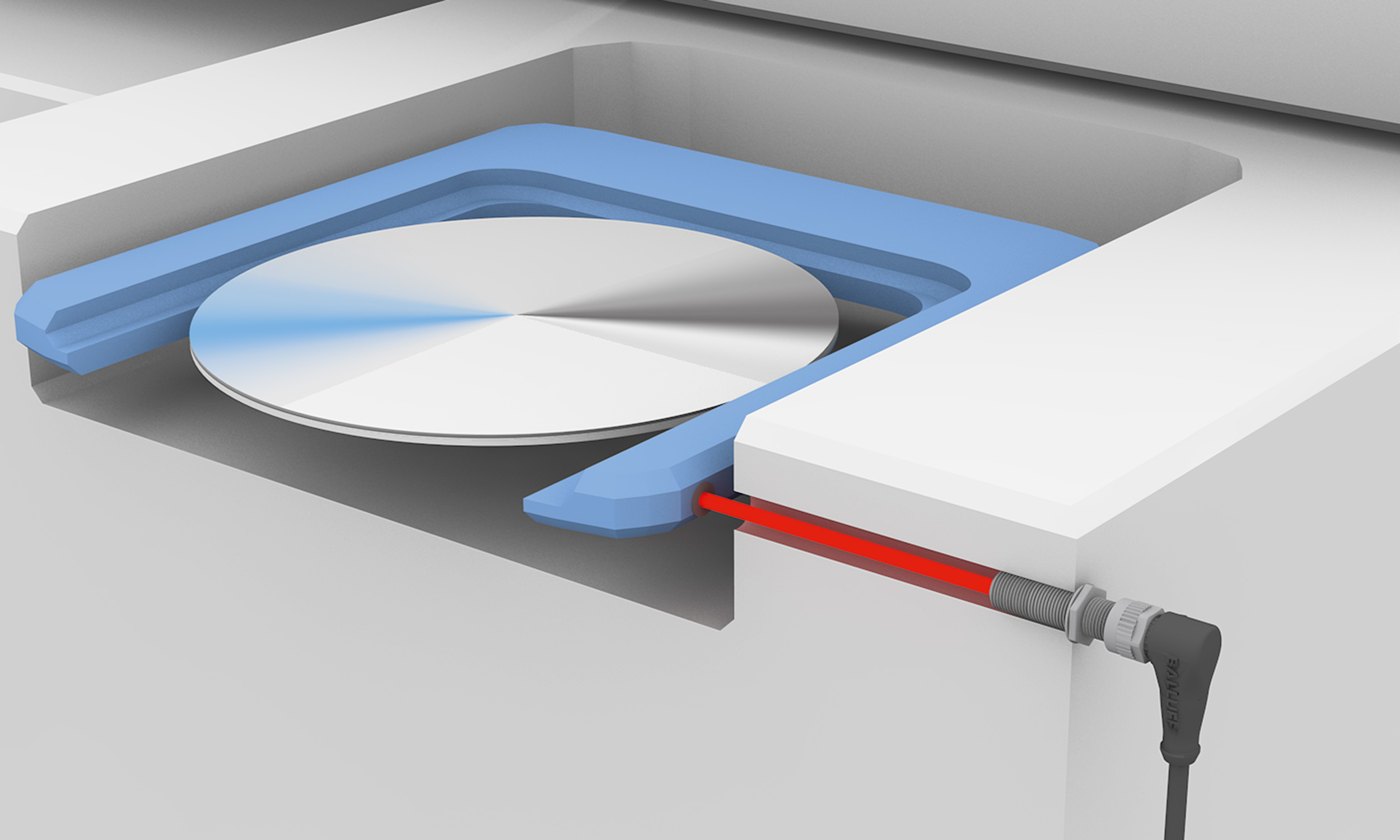
Wafer handling:
High precision even between process steps
For wafer handling in the EFEM module, such as on the end effector or the pre-aligner, Balluff provides you with high precision. Because only with extreme accuracy, wafers can be precisely positioned and reliably transported to feed them to each individual processing step.
Our sensors and systems are available in small designs for easy integration into the machine. For particularly difficult conditions, we also adapt our technology individually to your requirements.
The non-contact measuring principles avoid abrasion so that the clean room class is guaranteed throughout the entire process. Use the reliable monitoring of wafer handling and safeguard your process.
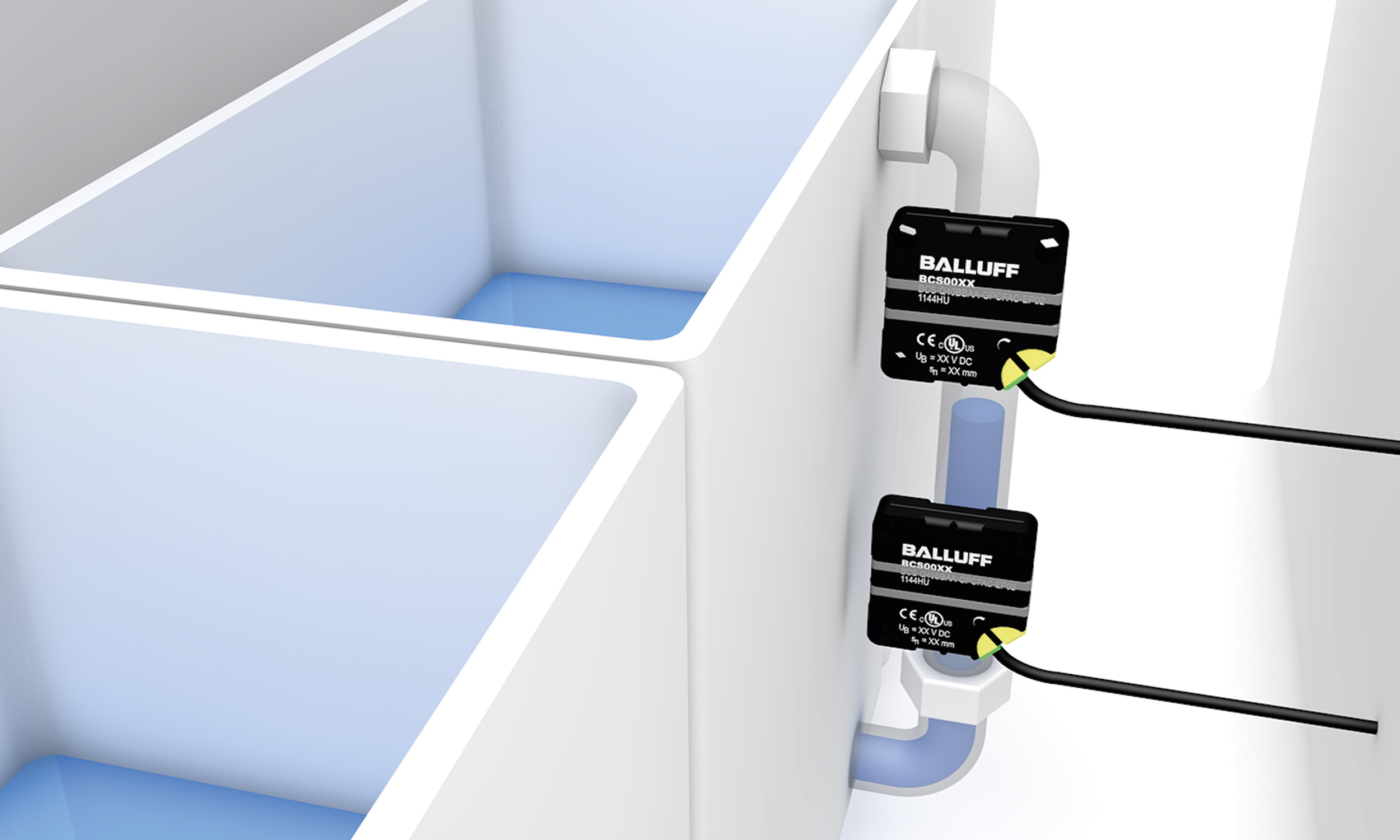
Wafer processing:
Operate reliably in a chemical environment
To meet the special requirements of semiconductor production, Balluff provides you with optimum solutions for processes in wet chemistry. Special PTFE housings enable reliable level control such as during etching, wafer cleaning or coating and developing in lithography. Our temperature sensors ensure that the process temperature is also correct. Contact sensors allow you to reliably monitor temperatures during wafer processing.
With our sensors, you can also control the valve stroke during wafer processing so that you can produce homogeneous and ideal layers during depositing.
![]()
Carrier handling:
Exact positioning without contact
Balluff systems support precise and efficient carrier handling, whether the carrier is a FOUP or a SMIF pod. With our systems, you can monitor the movements of the AMHS during fully automatic carrier transportation. And they do this extremely reliably, both on short distances with RGVs and on long distances with OHVs.
At the same time, the non-contact systems ensure precise positioning. This means that your wafers can be fed safely to each processing step. Friction and breakage are not a problem.
Balluff systems also guarantee consistent traceability. These ensure that the carrier position is documented in real time.
Vacuum applications:
To support process reliability
In the semiconductor industry, wafers are often processed in vacuum environments to ensure a clean and contamination-free environment.
Sensors from Balluff are characterized by outstanding properties and design features that allow them to be used directly in a vacuum. For example, for alignment on the fly in the vacuum lock or for checking the presence of wafers. We offer screw-in versions with a sealing function and sensors for installation directly in a high vacuum. We use outgassing-optimized materials to ensure process reliability. At your request, we can also manufacture the sensors in the materials you specify. The signals from the sensors are safely routed out via electrical cables using cable bushings.
Highlight products for the semiconductor industry
Discover specialized products that have been developed for the requirements of the semiconductor industry. Whether through precision in wafer mapping or through particularly high robustness for monitoring ALD valves, our products help you to increase your machine availability and ensure product quality.
Let us help you get the best out of your systems
Downloads
-
Industry brochure semiconductor industry
-
Custom Design and Engineering – custom specific camera and sensor solutions
-
Inductive high temperature sensors in Ø 5 mm housing for tight spaces
-
Mapping Sensor – delivering precision in the smallest possible space
-
BGL minislot miniaturized fork sensors from Balluff – flexible in the smallest space
-
Micromote – high optical performance in the smallest space